Online shopMy Plansee
Homepage
Online shopMy Plansee
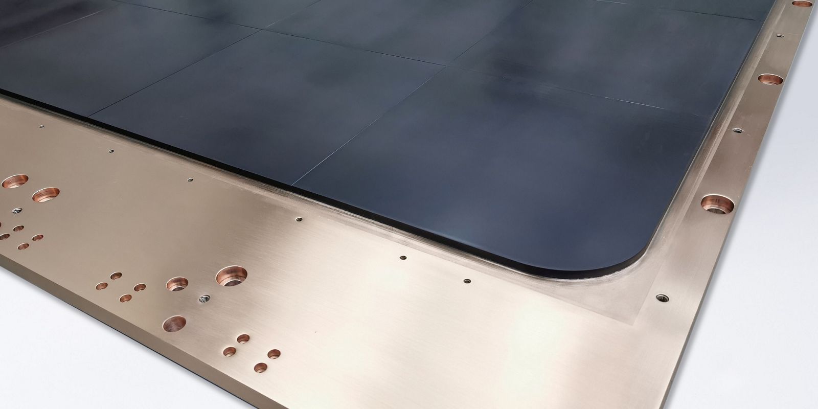
MoOxide sputtering target

Molybdenum oxide sputtering targets

Whether it's to reliably separate subpixels, elegantly cover conductor tracks or prevent troublesome reflections of the ambient light, molybdenum oxide layers have numerous applications in modern flat screens thanks to their low optical reflection. We provide molybdenum oxide as planar targets in various chemical compositions to produce these layers. To adjust the etchability and chemical resistance of the MoOx layers, molybdenum oxide is doped with further metallic elements.

Your advantages at a glance:

  • High purity
    > 99.9%

  • Homogeneous microstructure and chemical composition

  • Variable composition

  • Electrical conductivity

Download our product specifications:

MoOxTa8 sputtering target specification

The most important properties at a glance

Density [%] ≥ 95
Purity [%] > 99.9
Thermal coefficient of expansion [ppm/K] 5
Thermal conductivity [W/(m-K)] 4 - 6
Electrical conductivity [S/cm] 120 - 1100

Molybdenum oxide applications in screens

Narrow-bezel displays and touch screens: coverage of conductor tracks

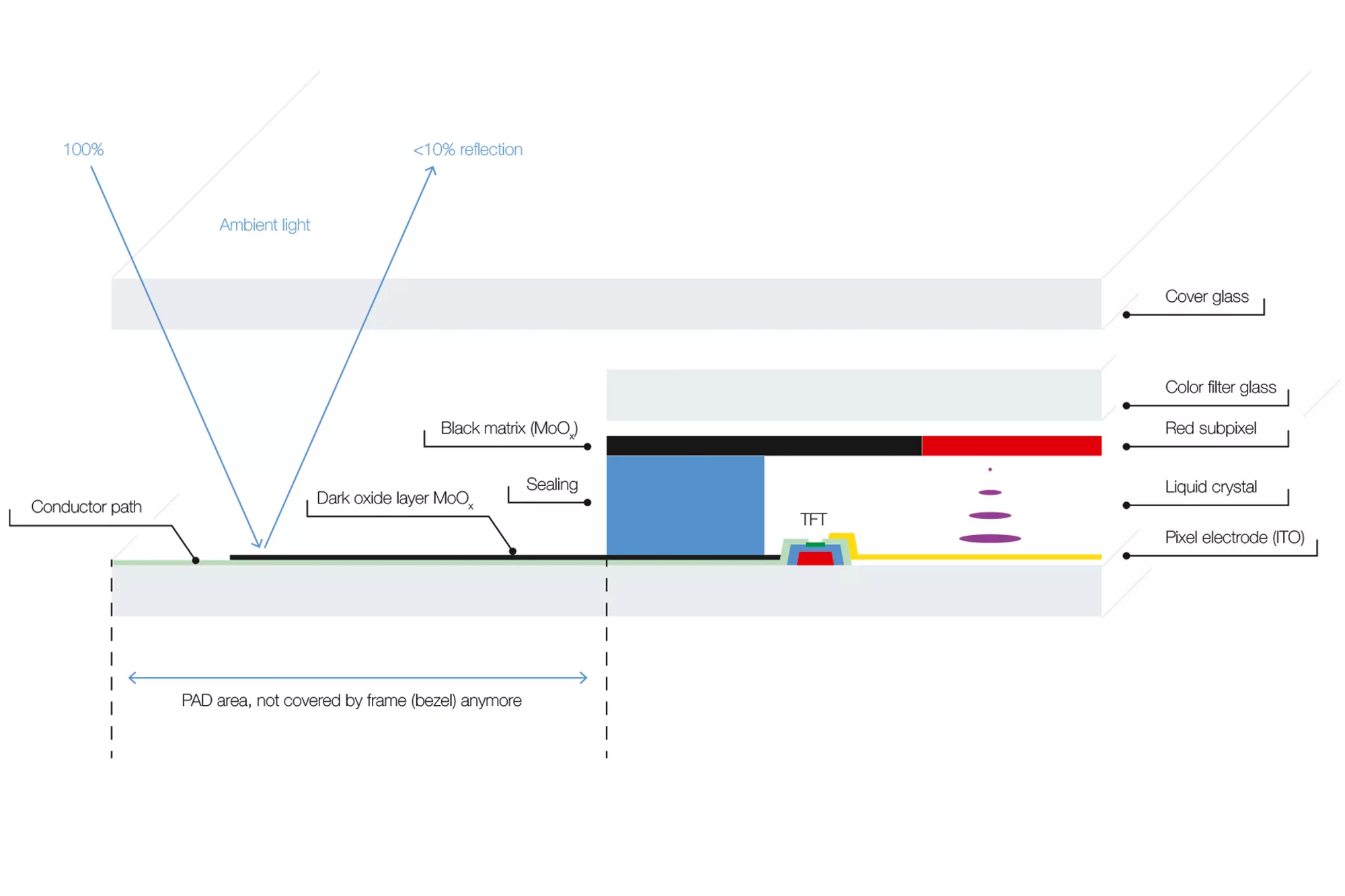
Modern desktop monitors and large TV displays often do not feature a plastic frame - the so-called bezel. This not only looks elegant but enables multiple screens to be placed together to form a large display. The missing plastic frame does mean, however, that the highly reflective conductor tracks made of molybdenum, aluminum or copper on the TFT glass are not covered. This is where an additional MoOx anti-reflection layer comes in. Whereas metal molybdenum reflects around 60% of the incident light, an MoOx layer of the same thickness reflects less than 6% (at 550 nm). This provides excellent shielding for the conductor tracks.

Mo oxide layer

Cross-section: how a molybdenum oxide layer covers the conductor tracks in narrow-bezel screens (= dark oxide layer).

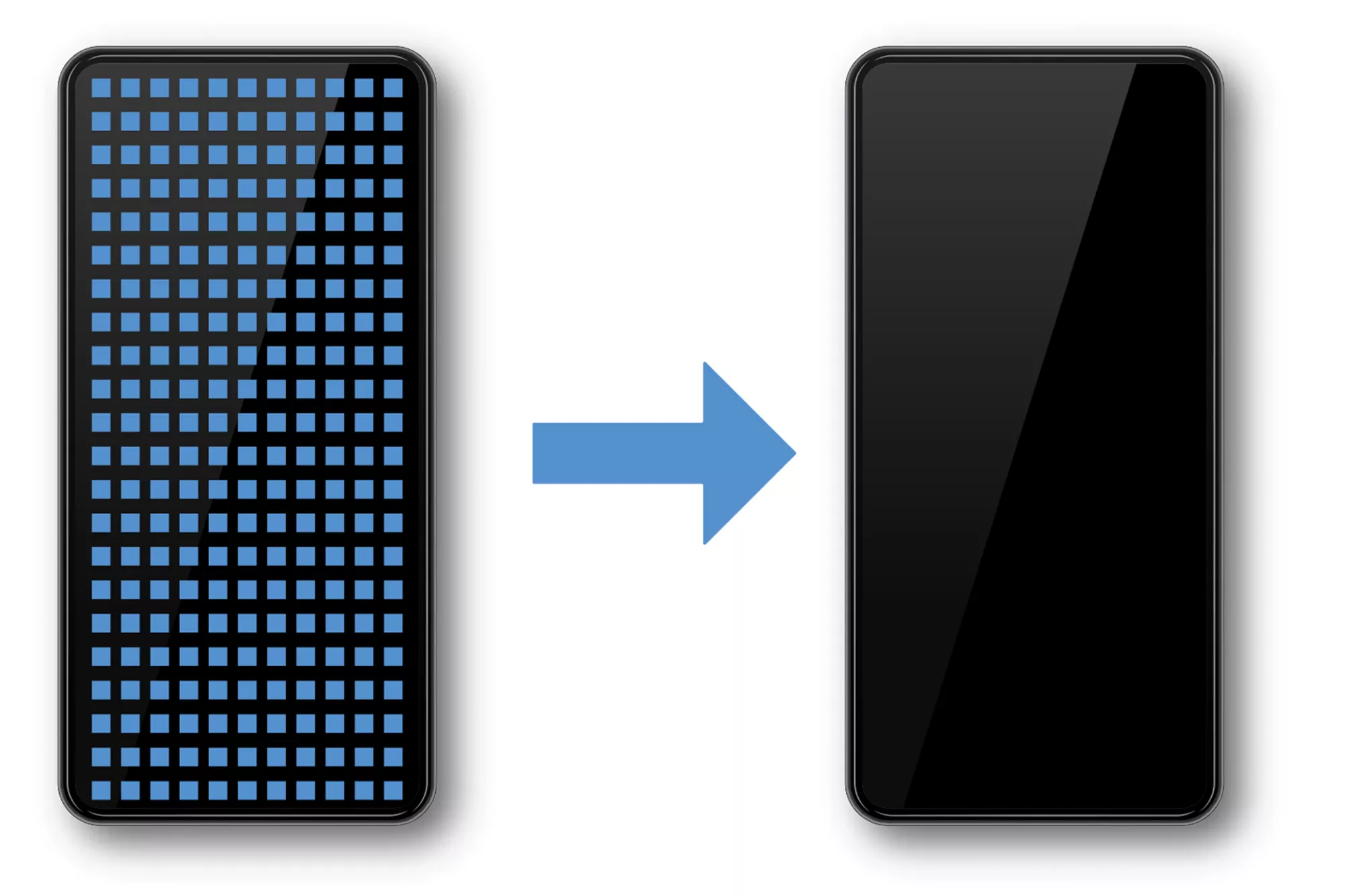
In touch screens, a thin PVD layer of molybdenum oxide prevents unwanted reflections of metallic surfaces (metal bridges) with capacitive tactile sensors.

Mo oxide layer smartphone

Tactile sensors in touch screens become invisible when coated with molybdenum oxide.

OLED: Reflection protection and electrode in one

When ambient light hits OLED displays, the molybdenum layers of the TFT metallization (gate, source/drain electrodes) reflect the ambient light, thereby reducing the contrast of the display. Circular polarization filters are used to prevent these unwanted reflections. They do reduce the reflection of the electrode but also reduce the light yield of the display. As MoOx absorbs light extremely well and is also electrically conductive, this material is particularly suitable as an anti-reflective layer for the TFT metallization. Using MoOx allows OLED manufacturers to dispense with the polarization layer.

Transparent molybdenum oxide layers for OLED and solar cell technology

Transparent MoOx layers represent another area of application. By adding oxygen during the coating process, the oxygen content of the layers can be adjusted up to a stoichiometry of MoO3. These layers have special electronic properties, in particular a high electron work function. Transparent MoOx layers can therefore be used in OLED technology as so-called "hole injection layers" (HIL). In thin-film solar cells based on CIGS and CdTe, MoOx layers are described and used as a component in the back contact and as a barrier layer (e.g., against selenization). Organic solar cells also benefit from additional layers of MoO3.

Further details can be found in the article "Thin-film metal oxides in organic semiconductor devices: their electronic structures, work functions and interfaces" by Nature Research.

To the publication

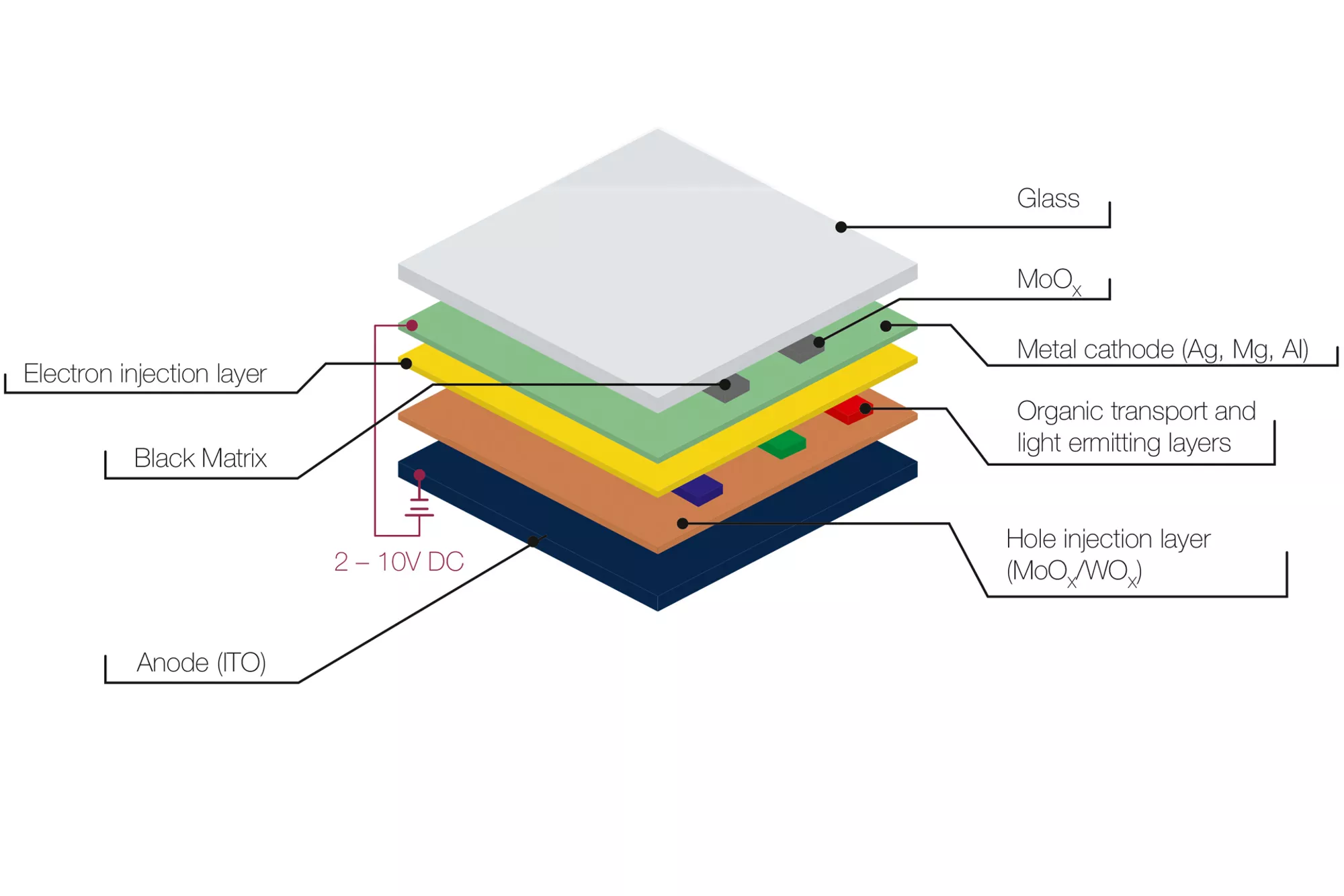
Simplified diagram of the structure of the RBG pixels in an OLED display:

Mo oxide layer OLED display

Simplified diagram of the active layers in an OLED display

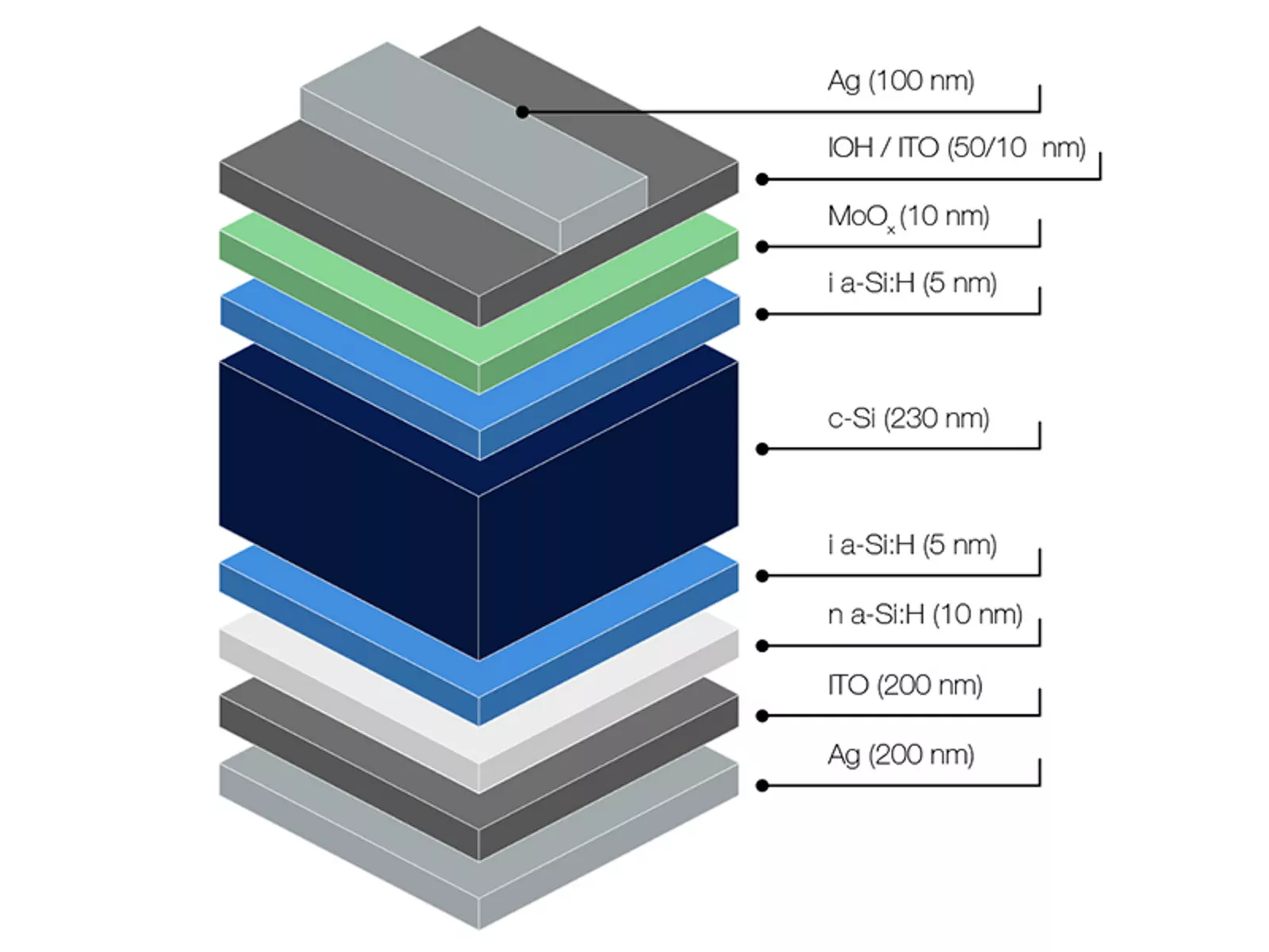
Transparent MoOx layers are also used in high-efficiency Heterojunction Si solar cells. Researchers at the EPFL Institute in Lausanne have released a publication on this subject, entitled "Toward Annealing‐Stable Molybdenum‐Oxide‐Based Hole‐Selective Contacts For Silicon Photovoltaics - Essig - 2018 - Solar RRL - Wiley Online Library".

To the publication
Mo oxide layer solar cell
Schematic representation of a MoOx/a-Si:H/c-Si solar cell structure

The suitability of molybdenum oxide layers for use in water splitting (photocatalytic production of hydrogen) in gas sensors, catalysts or thin-film batteries are further interesting fields of application that are currently the focus of scientific investigations.

Center of expertise for new coating solutions

In the PVD coating process, everything must be perfectly matched. It is only if all process parameters are perfectly matched that the layer that meets the exact customer-specific requirements can be produced. We carry out sputtering under practical conditions in our PVD application laboratory. Our team of developers produces layers and analyzes them in detail according to defined specifications. We test the coating properties of molybdenum oxide in our own coating lab. We'll be happy to offer advice on the various material compositions, film thicknesses, and process parameters.

We have already applied for several patents for the manufacture and properties of our molybdenum oxide sputtering targets.

Further articles on the subject:

Thin-film metal oxides in organic semiconductor devices: their electronic structures, work functions and interfaces

To the publication

Toward Annealing‐Stable Molybdenum‐Oxide‐Based Hole‐Selective Contacts For Silicon Photovoltaics - Essig - 2018 - Solar RRL - Wiley Online Library

To the publication

Other products for the coating industry: