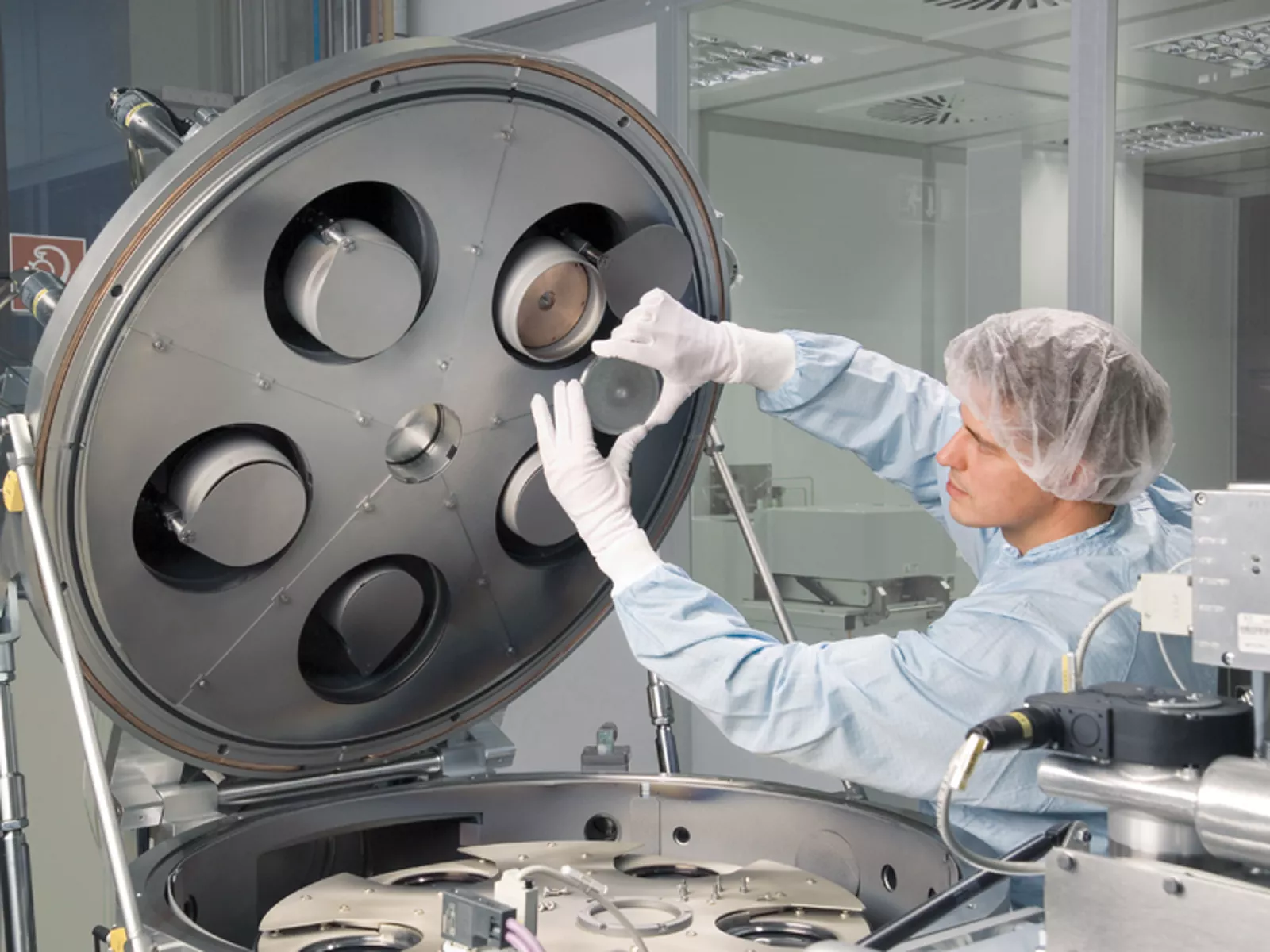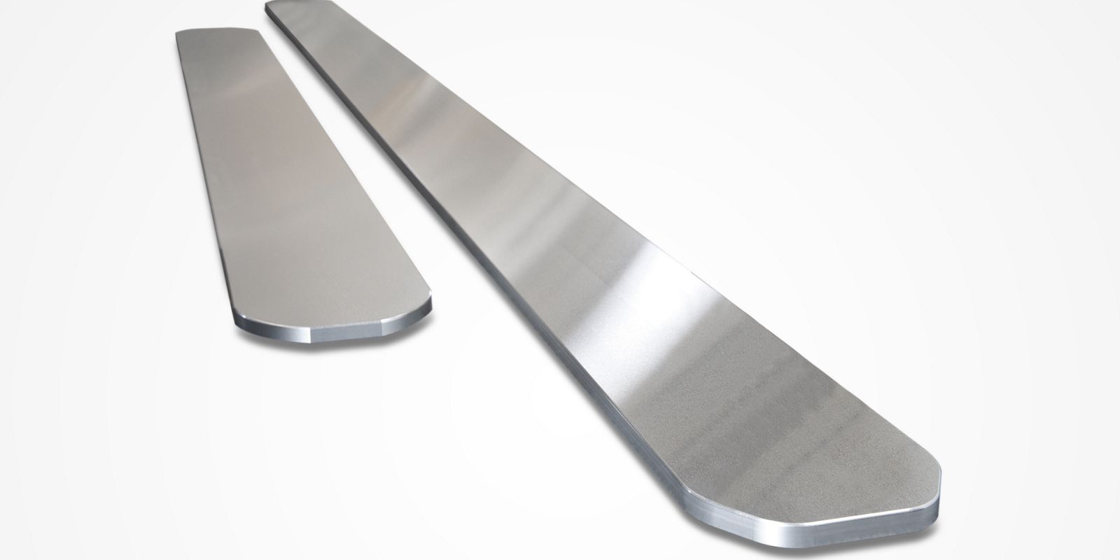
In the PVD coating process, everything must be perfectly matched. It is only if all process parameters are perfectly matched that the layer that suits the customer's exact requirements can be produced. We carry out sputtering under real-life conditions in our PVD application laboratory. Our team of developers produces layers and analyzes them in detail according to defined specifications. New coating materials are developed in a short period of time in cooperation with our customers and development partners. Having worked with system manufacturers and OEMs for several years, we are directly involved in the latest developments and optimizations. We coat many of our products such as semiconductor base plates and rotating X-ray anodes in-house using the PVD, CVD, APS, and VPS coating processes.


