Online shopMy Plansee
Homepage
Online shopMy Plansee
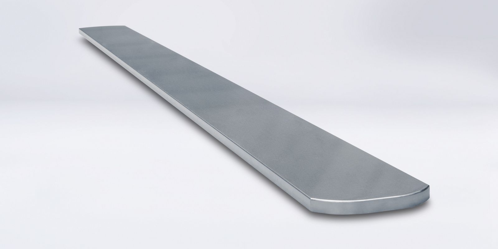
W sputtering target

Tungsten sputtering targets

Tungsten layers are components of thin-film transistors in TFT-LCD screens. They are used when large screen formats, a particularly high image definition, and optimized contrasts are required. Tungsten targets are also used in microelectronics, for example for creating layers in frequency filters (SAW/surface acoustic wave filter, BAW/bulk acoustic wave filter). Other applications for tungsten targets include diffusion barriers made of tungsten-nitride, conductor tracks in microelectronic components as well as reactively sputtered transparent layers made from tungsten oxide for OLED displays and for use in electrochemistry.

Your advantages at a glance:

  • High purity
    > 99.97%

  • Maximum density
    > 99.5%

  • Center of expertise for new coating solutions

  • Homogeneous microstructure

Download our product specifications:

W sputtering target specification

How are tungsten layers produced?

During the magnetron sputtering process (PVD process), tiny metal particles are released from the sputtering targets, which settle as a thin film on the material - the so-called substrate - to be coated. This coating process is a cost-effective and fast coating process in which all materials must satisfy the most stringent quality criteria.

Maximum purity

Our targets fulfill the most stringent purity requirements. The main advantages: excellent electrical conductivity of the layer and minimum particle formation during the PVD process. Metal and non-metal impurities in the sputtering target are transferred to the sputtered functional layer, thereby affecting its function or causing particle formation in the PVD process (the so-called arcing effect). We guarantee that our tungsten targets are at least 99.97% pure. The typical purity of our tungsten targets is even higher at 99.99%. This is how we guarantee that the layers produced satisfy the stringent requirements particularly for use in microelectronics.

Maximum density and homogeneous microstructure

Tungsten sputtering targets from Plansee are highly compressed by means of special forming processes. The advantage for the PVD coating process is homogeneous coating rates and improved coating properties. This results in improved efficiency and output in the production of thin films. Our powder metallurgical manufacturing process enables us to adjust the microstructure of the coating material to the specific application.

Center of expertise for new coating solutions

Plansee bonding shop

In the PVD process, everything must be perfectly matched. It is only if all process parameters are perfectly matched that the layer that meets the exact customer-specific requirements can be produced. We carry out sputtering under practical conditions in our PVD application laboratory. Our team of developers produces layers and analyzes them in detail according to defined specifications. New coating materials are developed in a short period of time in cooperation with our customers and numerous development partners. Having worked with system manufacturers and OEMs for several years, we are directly involved in the latest developments and optimizations.

Raw material supply from a single source

We house the entire value-added chain for our sputtering targets under one roof. From the raw material to the final product. Our in-house production encompasses both the development of new materials and the optimization of layers and coating processes. Sintering is the central process in our powder metallurgical manufacturing process. This is how we manufacture compact metal products from porous powder blanks. We produce tungsten planar targets in the world's largest hot-rolling mill for refractory metals. Following the machining process, we finalize the sputtering targets ready for installation in our local bonding shops.

Our customers have been relying on Plansee as an independent private company for an entire century. Reliability and continuity are just as important to us as they are to you. Especially when it comes to our raw material supply. With Global Tungsten & Powders and a shareholding in Molibdenos y Metales (Molymet), the Plansee Group covers all of the steps involved in tungsten and molybdenum processing. From producing the powder to powder metallurgical processes, all the way through the production of semifinished products and customer-specific components.

    Oxide
    Reduction
    Mixing alloys
    Pressing
    Sintering
    Forming
    Heat treatment
    Mechanical processing
    Bonding
    Quality assurance
    Recycling
OxideMolymet (Chile) is the world's largest processor of molybdenum ore concentrates and our main supplier of molybdenum trioxide. The Plansee Group holds a 21.15% share in Molymet. Global Tungsten & Powders (USA) is a division of the Plansee Group and our main supplier of tungsten metal powder.

Other products for the coating industry: